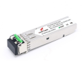
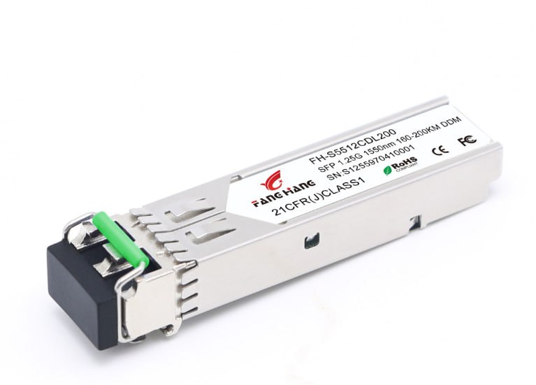
Empty FH-S5512CDL200

Акименко Евгений (Новосибирск)
Алексеев Никита (Москва)
Бадер Дарья (Новосибирск)
Бекетов Максим (Новосибирск)
Браун Захар (Новосибирск)
Бринева Анна (Москва)
Бубенов Максим (Новосибирск)
Буйнич Алексей (Новосибирск)
Бурдюгова Татьяна (Москва)
Бурмистров Игорь (Москва)
Васильева Татьяна (Москва)
Дашкина Ксения (Новосибирск)
Дудоров Дмитрий (Москва)
Жигульская Екатерина (Москва)
Ильиных Никита (Новосибирск)
Камышников Григорий (Новосибирск)
Каночкин Виталий (Москва)
Кириллова Маргарита (Новосибирск)
Клюй Вячеслав (Москва)
Козлов Дмитрий (Новосибирск)
Кузьмин Максим (Москва)
Ларин Алексей (Москва)
Ломоносова Екатерина (Новосибирск)
Лысенко Алексей (Москва)
Макаревич Евгений (Новосибирск)
Монтоев Анатолий (Новосибирск)
Мосин Михаил (Новосибирск)
Муртазин Камиль (Казань)
Наполов Илья (Москва)
Передерин Сергей (Новосибирск)
Поддубный Владислав (Москва)
Пучков Александр (Москва)
Пчелинская Светлана (Москва)
Рекун Антон (Москва)
Репьюк Алексей (Новосибирск )
Самойлов Иван (Новосибирск)
Сидоренко Никита (Новосибирск)
Степанов Артем (Москва)
Сутоцких Илья (Москва)
Сытый Александр (Москва)
Трифонов Артем (Новосибирск)
Ударцев Евгений (Новосибирск)
Фадин Дмитрий (Москва)
Файзрахманов Марат (Москва)
Чердынцев Артём (Москва)
Шатуха Егор (Москва)
Шаяхметов Илья (Новосибирск)
Щербаков Максим (Москва)
Краткое техническое описание (Datasheet)

www.fanghangtech.com 2015-08
FH-S5512CDL200
1.25G SFP 1550nm LC 200km DDMI
1st
Product Features
Support IEEE802.3 and Fiber Channel Applicable
Support 1.25G GbE and 1.0625G for Fiber-Channel
Support to 200km transmission on G.652 SMF
1550nm transmitter with EML laser
1550nm receiver with APD photo-detector
Low power consumption, < 1.5W
Digital Diagnostic Monitor Interface
Compliant with SFP MSA and SFF-8472
Very low EMI and excellent ESD protection
Operating case temperature: Commercial:0 to 70 °C
Applications
Gigabit Ethernet
Fiber Channel
Switch to Switch interface
Switched backplane applications
Router/Server interface
Other optical transmission systems
Ordering Information
Part Number
Output Power
Rec. Sens
Data Rate
Wavelength
Distance
FH-S5512CDL200
+4~ +7db
-34db
1.25/1.0625Gbps
1550nm
200KM

www.fanghangtech.com 2015-08
FH-S5512CDL200
1.25G SFP 1550nm LC 200km DDMI
2nd
General
FH-S5512CDL200 SFP transceivers are high performance, cost effective modules supporting dual data-rate of
1.25Gbps/1.0625Gbps and 200km transmission distance with SMF.The transceiver consists of three sections: a EML laser
transmitter, a APD photo-diode integrated with a trans-impedance preamplifier (TIA) and MCU control unit. All modules
satisfy class I laser safety requirements.The transceivers are compatible with SFP Multi-Source Agreement (MSA) and
SFF-8472. For further information, please refer to SFP MSA.
Absolute Maximum Ratings
Parameter
Symbol
Min.
Max.
Unit
Note
Supply Voltage
Vcc
-0.5
3.6
V
Storage Temperature
-40
85
°C
Relative Humidity
5
85
%
Note: Stress in excess of the maximum absolute ratings can cause permanent damage to the module
General Operating Characteristics
Parameter
Symbol
Min.
Typ.
Max.
Unit
Notes
Data Rate
Gigabit Ethernet
1.25
Gb/s
Fiber Channel
1.0625
Supply Voltage
Vcc
3.1
3.3
3.5
V
Supply Current
Icc
450
mA
Operating Case Temperature
Tc
0
70
℃

www.fanghangtech.com 2015-08
FH-S5512CDL200
1.25G SFP 1550nm LC 200km DDMI
3rd
Electrical Input/Output Characteristics
Parameter
Symbol
Min.
Typ
Max.
Unit
Note
Transmitter
Differential data input swing
VINPP
120
850
mVpp
1
Transmit Disable Voltage
VD
VCC-0.8
Vcc
V
Transmit Enable Voltage
VEN
0
0.8
Input differential impedance
Rin
100
Ω
Receiver
Differential data output swing
Vout,pp
400
1000
mVpp
2
Output rise time and fall time
Tr, Tf
28
Ps
3
LOS asserted
VLOS_F
VCC-0.8
Vcc
V
4
LOS de-asserted
VLOS_N
0
0.8
V
4
1. Connected directly to TX data input pins. AC coupling from pins into laser driver IC.
2. Into 100Ω differential termination.
3. 20 – 80%. Measured with Module Compliance Test Board and OMA test pattern. Use of four 1’s and four 0’s sequence in the PRBS 9 is an
acceptable alternative.
4. LOS is an open collector output. Should be pulled up with 4.7kΩ – 10kΩ on the host board. Normal operation is logic 0; loss of signal is logic 1.

www.fanghangtech.com 2015-08
FH-S5512CDL200
1.25G SFP 1550nm LC 200km DDMI
4th
Optical Characteristics
Note 1) Measured at 1250 Mb/s with PRBS 223 – 1 NRZ test pattern.
2) Measured at 1250 Mb/s with PRBS 223 – 1 NRZ test pattern for BER < 1x10-12
Parameter
Symbol
Min.
Typical
Max.
Unit
Notes
Transmitter
Ave. Output Power (Enable)
Po
+5
+7
dBm
1
Extinction Ratio
ER
30
dB
1
Relative Intensity Noise
RIN
-128
dB/Hz
Wavelength Range
1530
1550
1565
nm
Spectral Width (RMS)
1
nm
Output Optical Eye
Compliant with IEEE802.3 z (class 1 aser safety)
Receiver
Operating Wavelength
1260
1550
1610
nm
Sensitivity
Pimin
-34
dBm
2
Min. Overload
Pimax
-7
dBm
LOS Assert
Pa
-45
dBm
LOS De-assert
Pd
-35
dBm
LOS Hysteresis
Pd-Pa
0.5
6
dB

www.fanghangtech.com 2015-08
FH-S5512CDL200
1.25G SFP 1550nm LC 200km DDMI
5th
Pin Definitions And Functions
Pin
Symbol
Name/Description
1
VEET [1]
Transmitter Ground
2
Tx_FAULT [2]
Transmitter Fault
3
Tx_DIS [3]
Transmitter Disable. Laser output disabled on high or open
4
SDA [2]
2-wire Serial Interface Data Line
5
SCL [2]
2-wire Serial Interface Clock Line
6
MOD_ABS [4]
Module Absent. Grounded within the module
7
RS0 [5]
Rate Select 0
8
RX_LOS [2]
Loss of Signal indication. Logic 0 indicates normal operation
9
RS1 [5]
Rate Select 1
10
VEER [1]
Receiver Ground
11
VEER [1]
Receiver Ground
12
RD-
Receiver Inverted DATA out. AC Coupled
13
RD+
Receiver DATA out. AC Coupled
14
VEER [1]
Receiver Ground
15
VCCR
Receiver Power Supply
16
VCCT
Transmitter Power Supply
17
VEET [1]
Transmitter Ground
18
TD+
Transmitter DATA in. AC Coupled
19
TD-
Transmitter Inverted DATA in. AC Coupled
20
VEET [1]
Transmitter Ground

www.fanghangtech.com 2015-08
FH-S5512CDL200
1.25G SFP 1550nm LC 200km DDMI
6th
1.Module circuit ground is isolated from module chassis ground within the module.
2.should be pulled up with 4.7k – 10k ohms on host board to a voltage between 3.15Vand 3.6V.
3.Tx_Disable is an input contact with a 4.7 kΩ to 10 kΩ pullup to VccT inside the module.
4.Mod_ABS is connected to VeeT or VeeR in the SFP+ module. The host may pull this contact up to Vcc_Host with a resistor in the range 4.7 kΩ to10
kΩ.Mod_ABS is asserted “High” when the SFP+ module is physically absent from a host slot.
5. RS0 and RS1 are module inputs and are pulled low to VeeT with > 30 kΩ resistors in the module.
Serial Interface for ID and DDM
SFP transceiver support the 2-wire serial communication protocol as defined in the SFP+ MSA. The standard SFP+
serial ID provides access to identification information that describes the transceiver’s capabilities, standard interfaces,
manufacturer, and other information. Additionally, This SFP+ transceivers provide an enhanced digital diagnostic
monitoring interface, which allows real-time access to device operating parameters such as transceiver temperature, laser
bias current, transmitted optical power, received optical power and transceiver supply voltage. It also defines a
sophisticated system of alarm and warning flags, which alerts end-users when particular operating parameters are outside
of a factory set normal range.
The SFP MSA defines a 256-byte memory map in EEPROM that is accessible over a 2-wire serial interface at the 8
bit address 1010000X(A0h), so the originally monitoring interface makes use of the 8 bit address(A2h), so the originally
defined serial ID memory map remains unchanged. The structure of the memory map is shown in Table1.
Table 1. Digital Diagnostic Memory Map (Specific Data Field Descriptions)

www.fanghangtech.com 2015-08
FH-S5512CDL200
1.25G SFP 1550nm LC 200km DDMI
7th
Typical Interface Circuit
Recommended power supply filter
Note:
Inductors with DC resistance of less than 1Ω should be used in order to maintain the required voltage at the SFP input pin with 3.3V supply
voltage. When the recommended supply filtering network is used, hot plugging of the SFP transceiver module will result in an inrush current
of no more than 30 mA greater than the steady state value

www.fanghangtech.com 2015-08
FH-S5512CDL200
1.25G SFP 1550nm LC 200km DDMI
8th
Package Dimensions
For More Information
FANG HANG TECH LIMITED
Add: Room 908, Jingyuan Building, 28 Bulong Rd, Longgang District, Shenzhen China
Tel: +86-755-89584520
Fax: +86-755-89584520
sales@fanghangtech.com
www.fanghangtech.com