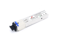
Empty FH-SB3512CDS40

Акименко Евгений (Новосибирск)
Алексеев Никита (Москва)
Бадер Дарья (Новосибирск)
Бекетов Максим (Новосибирск)
Браун Захар (Новосибирск)
Бринева Анна (Москва)
Бубенов Максим (Новосибирск)
Буйнич Алексей (Новосибирск)
Бурдюгова Татьяна (Москва)
Бурмистров Игорь (Москва)
Васильева Татьяна (Москва)
Дашкина Ксения (Новосибирск)
Дудоров Дмитрий (Москва)
Жигульская Екатерина (Москва)
Ильиных Никита (Новосибирск)
Камышников Григорий (Новосибирск)
Каночкин Виталий (Москва)
Кириллова Маргарита (Новосибирск)
Клюй Вячеслав (Москва)
Козлов Дмитрий (Новосибирск)
Кузьмин Максим (Москва)
Ларин Алексей (Москва)
Ломоносова Екатерина (Новосибирск)
Лысенко Алексей (Москва)
Макаревич Евгений (Новосибирск)
Монтоев Анатолий (Новосибирск)
Мосин Михаил (Новосибирск)
Муртазин Камиль (Казань)
Наполов Илья (Москва)
Передерин Сергей (Новосибирск)
Поддубный Владислав (Москва)
Пучков Александр (Москва)
Пчелинская Светлана (Москва)
Рекун Антон (Москва)
Репьюк Алексей (Новосибирск )
Самойлов Иван (Новосибирск)
Сидоренко Никита (Новосибирск)
Степанов Артем (Москва)
Сутоцких Илья (Москва)
Сытый Александр (Москва)
Трифонов Артем (Новосибирск)
Ударцев Евгений (Новосибирск)
Фадин Дмитрий (Москва)
Файзрахманов Марат (Москва)
Чердынцев Артём (Москва)
Шатуха Егор (Москва)
Шаяхметов Илья (Новосибирск)
Щербаков Максим (Москва)
Краткое техническое описание (Datasheet)

www.fanghangtech.com
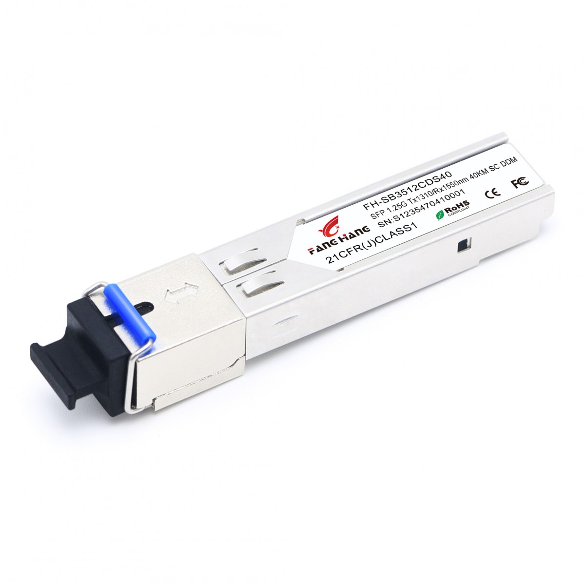
FH-SB3512CDS40
1.25G WDM TX1310/RX1550 40KM DDMI SC
1st
Product Features
Dual data-rate of 1.25Gbps/1.063Gbps operation
TX1310nm DFB laser
RX1550 PIN photo detector for 40km transmission
BIDI SC/UPC type pluggable optical interface
Compliant with SFP MSA and SFF-8472 with simplex SC receptacle
RoHS compliant and lead-free
Single +3.3V power supply
Support Digital Diagnostic Monitoring interface
Case operating temperature Commercial: 0°C to +70°C
Extended: -10°C to +80°C
Industrial: -40°C to +85°C
Applications
Gigabit Ethernet
Fiber Channel
Switch to Switch interface
Switched backplane applications
Router/Server interface
Other Optical Links
Ordering Information
Part Number
Output Power
Rec. Sens
Data Rate
Wavelength
Distance
FH-SB3512CDS40
FH-SB3512IDS40
-5 ~ 0 db
-22db
1.25G
TX1310/RX1550nm
40km

www.fanghangtech.com
FH-SB3512CDS40
1.25G WDM TX1310/RX1550 40KM DDMI SC
2nd
General
FH-SB3512CDS40 SFP-BIDI transceivers are high performance, cost effective modules supporting dual data-rate of
1.25Gbps/1.0625Gbps and 40km transmission distance with SMF.
The transceiver consists of three sections: a DFB laser transmitter, a PIN photodiode integrated with a
trans-impedance preamplifier (TIA) and MCU control unit. All modules satisfy class I laser safety requirements.
The transceivers are compatible with SFP Multi-Source Agreement (MSA) and SFF-8472. For further information,
please refer to SFP MSA.
Absolute Maximum Ratings
Parameter
Symbol
Min.
Max.
Unit
Note
Supply Voltage
Vcc
-0.5
4.0
V
Storage Temperature
-40
85
°C
Relative Humidity
85
%
Note: Stress in excess of the maximum absolute ratings can cause permanent damage to the module
General Operating Characteristics
Parameter
Symbol
Min.
Typ
Max.
Unit
Note
Data Rate
1250
Gb/s
Supply Voltage
Vcc
3.13
3.3
3.47
V
Supply Current
Icc5
220
mA
Operating Case Temp.
Tc
0
70
°C

www.fanghangtech.com
FH-SB3512CDS40
1.25G WDM TX1310/RX1550 40KM DDMI SC
3rd
Electrical Input/Output Characteristics
Parameter
Symbol
Min.
Typ
Max.
Unit
Note
Transmitter
Diff. input voltage swing
120
820
mVpp
1
Tx Disable input
H
VIH
2.0
Vcc+0.3
V
L
VIL
0
0.8
Tx Fault output
H
VOH
2.0
Vcc+0.3
V
2
L
VOL
0
0.8
Input Diff. Impedance
Zin
100
Ω
Receiver
Diff. output voltage swing
340
650
800
mVpp
3
Rx LOS Output
H
VOH
2.0
Vcc+0.3
V
2
L
VOL
0
0.8
Note 1 TD+/- are internally AC coupled with 100Ω differential termination inside the module.
2 Tx Fault and Rx LOS are open collector outputs, which should be pulled up with 4.7k to 10kΩ resistors on the host board.
Pull up voltage between 2.0V and Vcc+0.3V.
3 RD+/- outputs are internally AC coupled, and should be terminated with 100Ω (differential) at the user SERDES.

www.fanghangtech.com
FH-SB3512CDS40
1.25G WDM TX1310/RX1550 40KM DDMI SC
4th
Optical Characteristics
Parameter
Symbol
Min.
Typ
Max.
Unit
Note
Transmitter
Operating Wavelength
λC
1270
1310
1360
nm
Ave. output power (Enabled)
Po
-5
0
dBm
1
Extinction Ratio
ER
9
dB
1
RMS spectral width
Δλ
4
nm
Rise/Fall time (20%~80%)
Tr/Tf
0.26
ps
2
Output Eye Mask
Compliant with IEEE802.3 z (class 1 laser safety)
Receiver
Operating Wavelength
1530
1550
1570
nm
Sensitivity
Psen
-22
dBm
3
Min. overload
Pimax
-3
dBm
LOS Assert
Pa
-35
dBm
LOS De-assert
Pd
-23
dBm
4
LOS Hysteresis
Pd-Pa
0.5
6
dB
Note 1 Measure at 2^23-1 NRZ PRBS pattern
2 Transmitter eye mask definition
3 Measured with Light source 1550nm , ER=9dB; BER =<10^-12 @PRBS=2^23-1 NRZ.
4 When LOS de-asserted, the RX data+/- output is signal output.

www.fanghangtech.com
FH-SB3512CDS40
1.25G WDM TX1310/RX1550 40KM DDMI SC
5th
Pin Definitions And Function
PIN
Name
Function
Notes
1
VeeT
Tx ground
2
Tx Fault
Tx fault indication, Open Collector Output, active “H”
1
3
Tx Disable
LVTTL Input, internal pull-up, Tx disabled on “H”
2
4
MOD-DEF2
2 wire serial interface data input/output (SDA)
3
5
MOD-DEF1
2 wire serial interface clock input (SCL)
3
6
MOD-DEF0
Model present indication
3
7
Rate select
No connection
8
LOS
Rx loss of signal, Open Collector Output, active “H”
4
9
VeeR
Rx ground
10
VeeR
Rx ground
11
VeeR
Rx ground
12
RD-
Inverse received data out
5
13
RD+
Received data out
5
14
VeeR
Rx ground
15
VccR
Rx power supply
16
VccT
Tx power supply
17
VeeT
Tx ground
18
TD+
Transmit data in
6
19
TD-
Inverse transmit data in
6
20
VeeT
Tx ground

www.fanghangtech.com
FH-SB3512CDS40
1.25G WDM TX1310/RX1550 40KM DDMI SC
6th
Notes: 1) When high, this output indicates a laser fault of some kind. Low indicates normal operation. And should be pulled up with a
4.7 – 10KΩ resistor on the host board.
2) TX disable is an input that is used to shut down the transmitter optical output. It is pulled up within the module with a 4.7 – 10KΩ
resistor. Its states are:
Low (0 – 0.8V): Transmitter on (>0.8, < 2.0V): Undefined
High (2.0V~Vcc+0.3V): Transmitter Disabled Open: Transmitter Disabled
3) Mod-Def 0,1,2. These are the module definition pins. They should be pulled up with a 4.7K – 10KΩ resistor on the host board.
The pull-up voltage shall be VccT or VccR.
Mod-Def 0 has been grounded by the module to indicate that the module is present
Mod-Def 1 is the clock line of two wire serial interface for serial ID
Mod-Def 2 is the data line of two wire serial interface for serial ID
4) When high, this output indicates loss of signal (LOS). Low indicates normal operation.
5) RD+/-: These are the differential receiver outputs. They are AC coupled 100Ω differential lines which should be terminated with
100Ω (differential) at the user SERDES. The AC coupling is done inside the module and is thus not required on the host board.
6) TD+/-: These are the differential transmitter inputs. They are AC-coupled, differential lines with 100Ω differential termination
inside the module. The AC coupling is done inside the module and is thus not required on the host board.
Diagnostics
Parameter
Range
Unit
Accuracy
Calibration
Temperature
0 to +70 -40 to +85
°C
±3°C
Internal/ External
Voltage
3.0 to 3.6
V
±3%
Internal/ External
Bias Current
2 to 80
mA
±10%
Internal/ External
TX Power
-11 to -1
dBm
±3dB
Internal/ External
RX Power
-25 to 0
dBm
±3dB
Internal/ External